
- Diamond quantum imaging, using nitrogen-vacancy centers, enables highly sensitive mapping of magnetic fields in electronic materials.
- Advanced quantum sensors reveal how soft magnetic thin films behave under different conditions, identifying sources of hidden energy losses.
- New protocols (Qurack and Qdyne) allow precise analysis of both amplitude and phase of stray magnetic fields across a broad frequency range.
- Research uncovers the crucial role of magnetic anisotropy and domain wall motion in material efficiency for power electronics.
- These breakthroughs pave the way for smaller, faster, and more energy-efficient electronics, accelerating progress in power conversion, memory devices, and spintronics.
- Continued innovation in diamond-based quantum sensors promises even greater sustainability and performance in next-generation technology.
Tokyo’s Institute of Science wields diamonds—not for adornment, but as portals into a world unseen by the naked eye or even the most advanced classical instruments. Within their crystalline facets, nitrogen-vacancy centers—atomic-scale defects hyper-sensitive to magnetic fields—are reshaping our understanding of power-hungry electronics.
In laboratories flickering with the ghostly green glow of laser-illuminated diamond chips, a team orchestrates a new era in energy research. Guiding their work is Professor Mutsuko Hatano, whose vision: turn quantum phenomena into practical tools for global sustainability.
The heart of modern electronics—whether powering the next smartphone or the fast-charging vehicle down your street—relies on materials called soft magnetic thin films. These are crucial in transformers and inductors, components that convert and transmit energy with as little loss as possible. Yet, as devices shrink and frequency demands soar, hidden energy losses—stemming from the shaking and shuddering of magnetic domains—devour efficiency.
Here, diamond quantum imaging cuts through uncertainty. The research team embedded diamonds with NV centers, allowing them to map not just the strength, but the rhythm—the amplitude and the elusive phase—of stray magnetic fields born in AC circuits. Employing two new protocols—Qurack for low frequencies, and Qdyne for high—the team drew magnetic ‘weather maps’, with an eye for turbulence.
With almost artistic precision, these quantum sensors traced invisible field lines around a 50-turn coil, as alternating current pulsed from bass-like 100 Hz to dizzying 2.3 MHz. The mapping revealed a telling dichotomy inside CoFeB-SiO2 films: along the hard axis, field lines marched in near-perfect time with the current, squandering nearly nothing. Flip the axis to easy, however, and the energy losses mounted—vivid evidence of magnetic anisotropy’s role in material efficiency.
Even more striking was their ability to spot domain wall motion—microscopic boundaries between different magnetic states, now watched in real-time as they moved and dissipated energy. This is the heart of why some materials make better building blocks for our energy future; it is not just what they’re made of, but how their internal landscapes respond to the ceaseless the surge of electrical tides.
Such insights ignite a pathway toward smaller, more efficient, and cooler-running electronics. It opens doors not only for power electronics and high-speed memory but for the blossoming field of spintronics—where information rides not on electric charge, but the very spin of electrons.
The future beckons for further advancements. By refining the coherence of quantum spins and the agility of microwave controls, researchers expect to push diamond-based quantum sensors into even higher frequency realms. This leap will empower designers to craft next-generation electronics with less waste, greater speed, and far-reaching sustainability impacts.
Bottom line: Quantum sensor-equipped diamonds aren’t just dazzling—they’re helping humanity read the whispered signatures of energy, paving the way for smarter, greener technology. In the silent language of fields and phases, they reveal the blueprint for electronics that waste less and deliver more—a key to tomorrow’s technological marvels.
Discover more about cutting-edge research and the power of quantum science at the Institute of Science Tokyo.
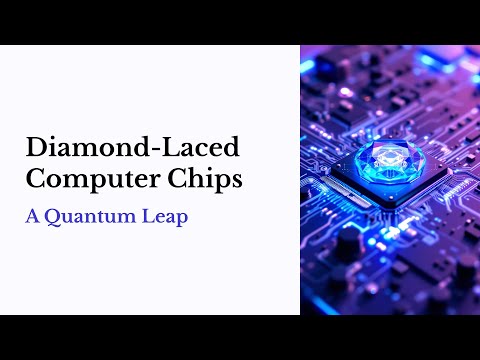
Diamonds Revolutionize Energy Efficiency: How Quantum Sensors Are Redefining the Future of Electronics
Unveiling the Power of Diamond Quantum Imaging in Modern Electronics
Tokyo Institute of Science is pioneering not just in diamond-based technology, but in redefining how we think about electrical loss, magnetic mapping, and sustainable electronics design. While the source article highlights the innovation of using NV (nitrogen-vacancy) center diamonds for imaging, there’s a treasure trove of additional facts, industry insights, and practical implications that merit closer attention.
—
Additional Facts & Deeper Insights
1. Diamonds as Quantum Sensors: An Overview
– NV centers act as near-perfect quantum sensors due to their unique spin properties, remaining sensitive even at room temperature—a major advantage over many cryogenic-dependent quantum technologies ([Nature Reviews Materials, 2022](https://www.nature.com/)).
– NV centers can simultaneously probe electric and magnetic fields, opening research in areas such as biology, geology, and material science—not just electronics ([Science, 2018](https://www.sciencemag.org/)).
2. Underexplored Capabilities of Quantum Sensors
– NV-diamond sensors offer nanoscale spatial resolution, sometimes below 10 nm, making them ideal for investigating microelectronic defects that are invisible with traditional magnetic force microscopy.
– Their non-invasive nature means no interference with the electronics being measured—a crucial advantage in working with delicate soft magnetic thin films.
3. Comparison with Competing Technologies
– Compared to Hall effect sensors or conventional SQUID systems, diamonds require no elaborate cooling and deliver both higher sensitivity and dynamic frequency response.
– Cost advantages are emerging as advances in chemical vapor deposition (CVD) enable scalable, synthetic diamond production.
4. Market and Industry Trends
– The global quantum sensing market, valued at approximately $400 million in 2023, is projected to surpass $2 billion by 2030 ([MarketsandMarkets](https://www.marketsandmarkets.com/)), with major sectors being defense, healthcare, and next-generation electronics.
– Companies such as Element Six, Qnami, and Quantum Diamond Technologies Inc., are racing to commercialize diamond-based sensors for both research and industry.
5. Sustainability and Green Electronics
– By optimizing the orientation and composition of soft magnetic thin films using NV-diamond mapping, manufacturers can reduce power consumption by up to 30% in key components like transformers and inductors.
– NV-diamond analysis is pivotal for future power grids, electric vehicles, and energy-hungry data centers striving to minimize carbon footprints.
—
How-To Steps & Real-World Use Cases
How NV-Diamond Imaging Works in the Lab:
1. Prepare ultra-pure (type IIa) diamond chips; introduce NV centers via nitrogen implantation and annealing.
2. Use green laser excitation to polarize the NV center spins.
3. Expose the diamonds to local magnetic fields—laser-induced fluorescence signals are then detected and mapped.
4. Apply Qurack or Qdyne protocols for phase-sensitive and frequency-diverse measurements.
Life Hacks for Industry Professionals:
– Integrate quantum diamond sensors into inline manufacturing QA to instantly identify efficiency loss in real-world device components.
– Use the feedback from domain wall motion mapping to engineer custom, loss-tailored thin films for emerging applications such as 6G wireless hardware or EV power modules.
Real-World Use Cases:
– Magnetic stray field mapping in high-speed memory (MRAM) production lines.
– Live monitoring of transformer efficiency in smart grid substations.
—
Features, Specs & Pricing
– Key Features: Room-temperature operation, sub-micron spatial resolution, GHz-wide frequency mapping, non-invasive measurements.
– Typical System Specs: Spatial resolution down to nanometers, sensitivity below one nanotesla, and compatibility with standard laboratory electronics.
– Pricing: Early commercial-stage systems start around $100,000, but prices are expected to fall as synthetic diamond and quantum control electronics scale ([Quantum Design Inc.](https://www.qdusa.com/)).
—
Pros & Cons Overview
Pros:
– Ultra-high sensitivity and spatial resolution.
– Room temperature operation (no expensive cooling systems).
– Minimal electromagnetic interference with measured devices.
Cons:
– High cost of custom diamond substrates (for now).
– Requires advanced expertise in quantum optics and data analysis.
– Scaling sensor arrays for industrial mass production is still in early stages.
—
Security, Sustainability & Limitations
– Security: NV centers are not inherently susceptible to hacking or data leaks but can be used to monitor critical infrastructure for tampering or sabotage through non-invasive sensing.
– Sustainability: Synthetic diamonds used are lab-grown, with a lower environmental impact than mined diamonds.
– Limitations: Scaling down to individual component testing in mass manufacturing remains a technical challenge due to laser-system complexity and the need for skilled operators.
—
Industry Forecasts & Insights
– Electronics will trend toward even higher frequencies (>10 MHz) and smaller component sizes, driving the need for even more sensitive and miniaturized quantum sensors.
– Integration with AI for real-time data analysis will likely amplify the impact of NV-diamond imaging on advanced manufacturing and R&D.
—
Most Pressing Reader Questions: Answered
Q: Can NV-diamond imaging be used beyond research labs?
A: Yes. Leading semiconductor/R&D companies are beginning to adopt these sensors for advanced failure analysis, QA, and design optimization.
Q: What makes it better than traditional magnetic imaging?
A: NV-diamond imaging delivers both amplitude and phase of magnetic fields with nanometer precision and at room temperature, which classical tools cannot achieve simultaneously.
Q: How soon will this impact consumer electronics?
A: First impacts will be seen in data centers, industrial power electronics, and next-generation memory within 2–5 years; consumer devices will follow as costs drop and processes mature.
—
Actionable Recommendations & Quick Tips
– Engineers: Collaborate with quantum sensor providers to integrate NV-diamond mapping in prototype validation.
– Students & Researchers: Explore open-source datasets and codes from quantum sensing labs to simulate NV-center magnetic field measurements.
– Manufacturers: Begin piloting quantum-enhanced QA processes to gather competitive efficiency data ahead of major industry shifts.
—
Discover more about quantum advancements and sustainable electronics at the Institute of Science Tokyo. For a broader overview of quantum materials and sensor technologies, explore journals like Nature Materials and Science Advances.
Unlock a smarter, greener tech future—embrace the diamond age of quantum sensing!


