Ultraviolet Lithography Equipment Manufacturing in 2025: Navigating Explosive Growth and Pioneering Innovations. Discover How Advanced Lithography is Shaping the Future of Semiconductor Fabrication.
- Executive Summary: 2025 Market Overview & Key Takeaways
- Industry Landscape: Major Players and Global Footprint
- Technology Evolution: Deep UV (DUV) vs. Extreme UV (EUV) Systems
- Market Size & Growth Forecast (2025–2030): CAGR and Revenue Projections
- Key Drivers: Semiconductor Demand, AI, and Advanced Node Scaling
- Challenges & Barriers: Supply Chain, Cost, and Technical Hurdles
- Regional Analysis: Asia-Pacific, North America, and Europe Trends
- Competitive Strategies: Innovation, Partnerships, and IP Leadership
- Emerging Applications: Beyond Semiconductors—MEMS, Photonics, and More
- Future Outlook: Roadmap to 2030 and Strategic Recommendations
- Sources & References
Executive Summary: 2025 Market Overview & Key Takeaways
The ultraviolet (UV) lithography equipment manufacturing sector is poised for significant developments in 2025, driven by the ongoing demand for advanced semiconductor devices and the push toward smaller process nodes. UV lithography, encompassing both deep ultraviolet (DUV) and extreme ultraviolet (EUV) technologies, remains a cornerstone of semiconductor fabrication, enabling the production of integrated circuits with ever-increasing density and performance.
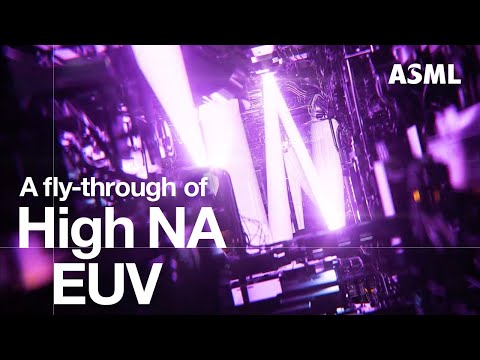
The market continues to be dominated by a small number of highly specialized manufacturers. ASML Holding NV stands as the undisputed leader in EUV lithography systems, supplying the majority of the world’s advanced EUV scanners to leading chipmakers. ASML’s EUV systems are critical for the production of chips at 5nm and below, and the company’s ongoing investments in high-NA (numerical aperture) EUV technology are expected to further extend the capabilities of UV lithography through 2025 and beyond. In 2024, ASML reported a robust order backlog, reflecting sustained demand from major foundries and integrated device manufacturers.
Other key players in the DUV segment include Nikon Corporation and Canon Inc., both of which continue to supply advanced DUV lithography equipment for mature and specialty nodes. These companies are focusing on incremental improvements in throughput, overlay accuracy, and cost efficiency to address the needs of memory, logic, and specialty semiconductor markets. Their equipment remains essential for applications where EUV adoption is not yet economically viable or technically required.
The supply chain for UV lithography equipment is highly complex, involving precision optics, light sources, and advanced materials. Suppliers such as Carl Zeiss AG provide critical optical components, while companies like Cymer (a subsidiary of ASML) are key providers of light sources for both DUV and EUV systems. The industry is also witnessing increased collaboration between equipment manufacturers and semiconductor foundries to accelerate process development and equipment qualification.
Looking ahead to 2025 and the following years, the UV lithography equipment market is expected to experience continued growth, fueled by the expansion of advanced semiconductor manufacturing in Asia, North America, and Europe. Geopolitical factors and government initiatives to localize semiconductor supply chains are prompting new investments in domestic manufacturing capacity, further boosting demand for state-of-the-art lithography tools. However, the sector faces challenges related to supply chain resilience, the high cost of EUV systems, and the technical complexity of next-generation lithography.
In summary, 2025 will see ultraviolet lithography equipment manufacturing remain at the heart of semiconductor innovation, with leading companies investing in new technologies and capacity to meet the evolving needs of the global electronics industry.
Industry Landscape: Major Players and Global Footprint
The ultraviolet (UV) lithography equipment manufacturing sector is a cornerstone of the global semiconductor industry, enabling the production of increasingly advanced integrated circuits. As of 2025, the industry is characterized by a concentrated group of major players, each with a significant global footprint and specialized technological capabilities.
The undisputed leader in the field is ASML Holding NV, headquartered in the Netherlands. ASML is the only company worldwide capable of producing extreme ultraviolet (EUV) lithography systems, which are essential for fabricating chips at the 5nm node and below. The company’s EUV systems are critical for leading-edge semiconductor manufacturing, and its customer base includes all major logic and memory chipmakers. ASML’s global presence is reinforced by manufacturing, R&D, and service centers in Europe, the United States, and Asia, supporting a robust supply chain and customer support network.
In the domain of deep ultraviolet (DUV) lithography, Nikon Corporation and Canon Inc., both based in Japan, remain prominent. These companies supply advanced DUV immersion and dry lithography systems, which are widely used for mature and mid-range semiconductor nodes. Nikon and Canon have established manufacturing and service operations across Asia, North America, and Europe, ensuring proximity to major foundries and integrated device manufacturers.
The global footprint of these manufacturers is further extended through strategic partnerships and collaborations with regional suppliers and technology institutes. For example, ASML’s supply chain includes critical component suppliers in Germany, the United States, and Japan, while Nikon and Canon maintain close ties with Japanese precision optics and robotics firms. This interconnected ecosystem supports rapid innovation and adaptation to evolving semiconductor requirements.
Looking ahead to the next few years, the industry landscape is expected to remain highly consolidated, with ASML maintaining its technological lead in EUV and high-NA EUV systems. However, both Nikon Corporation and Canon Inc. are investing in next-generation DUV and exploratory UV technologies to address the needs of specialty and legacy nodes, as well as emerging applications such as advanced packaging and heterogeneous integration. Regional initiatives in China and South Korea are also underway, aiming to localize certain aspects of lithography equipment manufacturing, though these efforts face significant technological and supply chain barriers.
Overall, the ultraviolet lithography equipment manufacturing sector in 2025 is defined by a small number of dominant players with extensive global operations, underpinned by deep technological expertise and complex international supply networks. The competitive landscape is expected to evolve gradually, with incremental advances in UV lithography technologies and ongoing efforts to diversify supply chains in response to geopolitical and market dynamics.
Technology Evolution: Deep UV (DUV) vs. Extreme UV (EUV) Systems
The ultraviolet lithography equipment manufacturing sector is undergoing a significant technological evolution, marked by the transition from Deep Ultraviolet (DUV) to Extreme Ultraviolet (EUV) systems. DUV lithography, which utilizes wavelengths of 193 nm (ArF) and 248 nm (KrF), has been the industry standard for decades, enabling the production of advanced semiconductor nodes down to 7 nm. However, as the demand for higher transistor densities and smaller feature sizes intensifies, DUV systems are reaching their physical and economic limits, prompting a shift toward EUV lithography, which operates at a much shorter wavelength of 13.5 nm.
As of 2025, ASML Holding NV remains the sole supplier of high-volume EUV lithography systems globally. The company’s EUV platforms, such as the Twinscan NXE and EXE series, are now critical for manufacturing leading-edge chips at 5 nm, 3 nm, and are being prepared for 2 nm and beyond. In 2024 and 2025, ASML is ramping up shipments of its latest High-NA EUV systems, which offer even greater resolution and productivity, supporting the industry’s roadmap for sub-2 nm nodes. The complexity and cost of EUV tools are substantial, with each system priced at over $200 million and comprising more than 100,000 parts, including advanced optics from Carl Zeiss AG and light sources from TRUMPF Group.
Despite the rapid adoption of EUV at the most advanced foundries, DUV lithography remains indispensable for mature nodes and for multi-patterning steps in advanced processes. Leading DUV equipment manufacturers include Nikon Corporation and Canon Inc., both of which continue to innovate in immersion and dry DUV scanners to serve memory, logic, and specialty device markets. In 2025, these companies are focusing on improving throughput, overlay accuracy, and cost efficiency to maintain competitiveness in a market where EUV is not yet economically viable for all applications.
Looking ahead, the outlook for ultraviolet lithography equipment manufacturing is shaped by the dual trajectory of DUV and EUV technologies. While EUV is expected to dominate leading-edge logic and memory production, DUV will persist in high-volume manufacturing for legacy nodes and emerging applications such as power devices and sensors. The ongoing evolution of both technologies is supported by robust R&D investments from equipment makers and their supply chain partners, ensuring that ultraviolet lithography remains the backbone of semiconductor fabrication through the remainder of the decade.
Market Size & Growth Forecast (2025–2030): CAGR and Revenue Projections
The ultraviolet (UV) lithography equipment manufacturing sector is poised for robust growth between 2025 and 2030, driven by escalating demand for advanced semiconductor devices, ongoing technology node shrinkage, and the proliferation of applications in artificial intelligence, 5G, and automotive electronics. The market is dominated by deep ultraviolet (DUV) and extreme ultraviolet (EUV) lithography systems, with EUV in particular representing the cutting edge for sub-7nm and sub-5nm chip production.
As of 2025, the global market for UV lithography equipment is estimated to be valued in the tens of billions of US dollars, with leading manufacturers reporting strong order backlogs and capacity expansion plans. ASML Holding NV, the undisputed leader in EUV lithography, continues to see surging demand for its EUV systems, which are essential for advanced logic and memory chip fabrication. The company’s financial disclosures indicate that its EUV system sales are expected to account for a growing share of its total revenue through 2030, reflecting the industry’s transition to more advanced nodes.
Other major players, such as Canon Inc. and Nikon Corporation, remain significant suppliers of DUV lithography equipment, serving both mature and emerging markets. These companies are investing in next-generation DUV platforms to address the needs of specialty and legacy nodes, which continue to represent a substantial portion of global semiconductor output.
Industry forecasts suggest a compound annual growth rate (CAGR) in the range of 7% to 10% for the UV lithography equipment market from 2025 to 2030. This growth is underpinned by aggressive capital expenditure plans from leading foundries and integrated device manufacturers, particularly in Asia and the United States. The expansion of advanced semiconductor fabrication facilities (“fabs”) by companies such as Taiwan Semiconductor Manufacturing Company and Samsung Electronics is expected to drive sustained demand for both EUV and advanced DUV systems.
Looking ahead, the market outlook remains positive, with revenue projections for UV lithography equipment manufacturers expected to surpass previous cycles. The ongoing evolution of chip architectures, coupled with the push for domestic semiconductor manufacturing in multiple regions, will likely reinforce the sector’s growth trajectory through 2030 and beyond.
Key Drivers: Semiconductor Demand, AI, and Advanced Node Scaling
The ultraviolet lithography equipment manufacturing sector is experiencing significant momentum in 2025, propelled by surging semiconductor demand, the proliferation of artificial intelligence (AI) applications, and the relentless drive toward advanced node scaling. These factors are converging to shape both the immediate and medium-term outlook for the industry.
Semiconductor demand remains robust, underpinned by the expansion of data centers, 5G infrastructure, automotive electronics, and consumer devices. The global push for digitalization and electrification is intensifying the need for high-performance, energy-efficient chips, which in turn necessitates advanced lithography solutions. Ultraviolet lithography, particularly extreme ultraviolet (EUV) technology, is now indispensable for fabricating chips at 5nm, 3nm, and even more advanced nodes. The world’s leading lithography equipment manufacturer, ASML Holding, continues to dominate the EUV market, supplying critical systems to major foundries and integrated device manufacturers worldwide.
AI is a transformative force, driving unprecedented requirements for computational power and memory bandwidth. The rapid adoption of generative AI, machine learning, and edge computing is accelerating the transition to smaller process nodes, where EUV lithography is essential for achieving the necessary transistor density and performance. Major chipmakers such as Taiwan Semiconductor Manufacturing Company (TSMC), Samsung Electronics, and Intel Corporation are investing heavily in EUV-enabled production lines to meet the surging demand for AI-optimized chips.
Advanced node scaling remains a central driver, as the industry roadmap targets sub-3nm technologies and beyond. The technical challenges of patterning at these dimensions require continuous innovation in lithography equipment, including higher numerical aperture (High-NA) EUV systems. ASML Holding is at the forefront, with its High-NA EUV platforms expected to enter pilot production in the next few years, enabling further scaling and improved chip performance. Suppliers of critical subsystems and materials, such as Carl Zeiss AG (optics) and ULVAC, Inc. (vacuum and deposition systems), are also ramping up capabilities to support this next generation of lithography tools.
Looking ahead, the ultraviolet lithography equipment manufacturing sector is poised for continued growth, with capital expenditures by leading foundries and IDMs expected to remain elevated through the decade. The interplay of semiconductor demand, AI-driven innovation, and advanced node scaling will sustain high utilization rates and drive further technological breakthroughs in lithography equipment.
Challenges & Barriers: Supply Chain, Cost, and Technical Hurdles
The manufacturing of ultraviolet (UV) lithography equipment, particularly for advanced semiconductor fabrication, faces significant challenges and barriers in 2025 and the coming years. These obstacles span the supply chain, cost structure, and technical complexity, each impacting the pace and scale of industry progress.
A primary challenge is the highly specialized and globalized supply chain required for UV lithography systems. Key components—such as high-precision optics, light sources, and ultra-clean mechatronic assemblies—are sourced from a limited number of suppliers worldwide. For example, the production of deep ultraviolet (DUV) and extreme ultraviolet (EUV) lithography machines relies on advanced optical components and light sources that only a handful of companies can manufacture to the necessary specifications. Disruptions in logistics, geopolitical tensions, or export controls can significantly delay equipment delivery and increase costs. In 2024 and 2025, ongoing trade restrictions and export controls, particularly between the United States, the Netherlands, and China, have further complicated the supply chain for critical lithography components, as seen in the export licensing requirements for advanced systems from ASML Holding N.V..
Cost remains a formidable barrier. The capital expenditure for state-of-the-art UV lithography equipment is immense, with EUV systems reportedly exceeding $200 million per unit. The high cost is driven by the extreme precision required in manufacturing, the need for ultra-clean environments, and the integration of complex subsystems such as high-power lasers and vacuum chambers. Only a few semiconductor manufacturers, such as Taiwan Semiconductor Manufacturing Company Limited and Samsung Electronics Co., Ltd., have the financial resources and technical expertise to acquire and operate these machines at scale. This concentration of capability limits broader industry access and slows the diffusion of advanced lithography technology.
Technical hurdles are equally daunting. The transition from DUV to EUV lithography, necessary for producing chips at 5 nm and below, introduces new engineering challenges. EUV systems require light sources operating at 13.5 nm, which are difficult to generate and maintain at the power levels needed for high-volume manufacturing. The development and maintenance of defect-free photomasks, high-reflectivity mirrors, and contamination-free environments are ongoing technical barriers. Canon Inc. and Nikon Corporation continue to invest in DUV and emerging EUV technologies, but the complexity of these systems means that even incremental improvements require significant R&D investment and time.
Looking ahead, the industry is expected to face continued supply chain vulnerabilities, escalating costs, and persistent technical challenges through at least the late 2020s. Addressing these barriers will require coordinated efforts among equipment manufacturers, component suppliers, and semiconductor foundries, as well as supportive policy frameworks in key regions.
Regional Analysis: Asia-Pacific, North America, and Europe Trends
The ultraviolet (UV) lithography equipment manufacturing sector is experiencing dynamic shifts across the Asia-Pacific, North America, and Europe regions in 2025, driven by semiconductor industry demand, government policies, and supply chain realignments. Each region exhibits distinct trends shaped by local capabilities, investment priorities, and strategic partnerships.
Asia-Pacific continues to dominate the global UV lithography equipment market, underpinned by the presence of major semiconductor foundries and a robust electronics manufacturing ecosystem. In 2025, countries such as Taiwan, South Korea, Japan, and increasingly China, are investing heavily in advanced lithography capabilities. Taiwan Semiconductor Manufacturing Company (TSMC) remains a pivotal player, expanding its capacity and collaborating with equipment suppliers to secure next-generation UV and extreme ultraviolet (EUV) systems. Samsung Electronics and SK Hynix in South Korea are also scaling up their investments, focusing on both deep ultraviolet (DUV) and EUV lithography to support memory and logic chip production. Japan’s Canon and Nikon continue to innovate in DUV equipment, maintaining a significant share in specialized lithography tools for mature nodes and niche applications.
In North America, the United States is reinforcing its position through policy support and domestic manufacturing initiatives. The CHIPS Act and related incentives are catalyzing investments in semiconductor fabrication and equipment manufacturing. Applied Materials and Lam Research are expanding their R&D and production capabilities, with a focus on supporting both domestic fabs and global customers. While the U.S. does not currently host leading-edge EUV tool manufacturing, it remains a critical supplier of subsystems, components, and process technologies essential for UV lithography equipment. Strategic partnerships with European and Asian firms are expected to intensify as the U.S. seeks to bolster its supply chain resilience.
Europe is home to the world’s only supplier of EUV lithography systems, ASML Holding, headquartered in the Netherlands. In 2025, ASML continues to ramp up production of both DUV and EUV systems to meet surging global demand, with a significant portion of its output destined for Asia-Pacific foundries. European governments are supporting semiconductor sovereignty initiatives, aiming to attract new fabs and strengthen the region’s position in the global value chain. Germany and France are emerging as focal points for new investments, leveraging their advanced engineering base and collaboration with ASML and other equipment suppliers.
Looking ahead, the Asia-Pacific region is expected to maintain its leadership in UV lithography equipment consumption, while North America and Europe focus on strategic autonomy and technology leadership. Cross-regional collaboration, supply chain diversification, and continued innovation in UV lithography technologies will shape the competitive landscape through the remainder of the decade.
Competitive Strategies: Innovation, Partnerships, and IP Leadership
The ultraviolet (UV) lithography equipment manufacturing sector is characterized by intense competition, with leading players deploying multifaceted strategies centered on innovation, strategic partnerships, and intellectual property (IP) leadership. As of 2025, the industry is witnessing accelerated advancements in both deep ultraviolet (DUV) and extreme ultraviolet (EUV) lithography, driven by the relentless demand for smaller, more powerful semiconductor devices.
Innovation remains the cornerstone of competitive strategy. ASML Holding NV continues to dominate the EUV lithography market, leveraging its unmatched expertise in high-NA (numerical aperture) EUV systems. The company’s ongoing R&D investments—exceeding €3 billion annually—are focused on enhancing throughput, yield, and resolution, with the first high-NA EUV systems expected to be delivered to leading chipmakers in 2025. These systems are critical for enabling sub-2nm process nodes, a key milestone for the semiconductor roadmap.
Strategic partnerships are increasingly vital for technology co-development and supply chain resilience. ASML Holding NV collaborates closely with key suppliers such as Carl Zeiss AG for precision optics and Cymer (a subsidiary of ASML Holding NV) for light sources. These alliances ensure the integration of cutting-edge components and the rapid scaling of new technologies. Meanwhile, Nikon Corporation and Canon Inc. remain significant players in the DUV segment, focusing on immersion lithography and advanced overlay solutions. Both companies are investing in joint ventures and research collaborations to maintain relevance as the industry transitions toward EUV.
IP leadership is a critical differentiator, with patent portfolios serving both as defensive shields and as leverage in cross-licensing negotiations. ASML Holding NV holds thousands of patents related to EUV and DUV technologies, reinforcing its market position and deterring new entrants. Nikon Corporation and Canon Inc. also maintain robust IP portfolios, particularly in optics and system integration, and have a history of litigation and settlements that shape the competitive landscape.
Looking ahead, the competitive dynamics in UV lithography equipment manufacturing are expected to intensify through 2025 and beyond. The race to commercialize next-generation EUV systems, secure critical supply chain partnerships, and expand IP portfolios will define industry leadership. Companies that can successfully integrate innovation, collaboration, and IP strategy are poised to capture the growing demand for advanced semiconductor manufacturing equipment.
Emerging Applications: Beyond Semiconductors—MEMS, Photonics, and More
Ultraviolet (UV) lithography equipment, long synonymous with semiconductor manufacturing, is increasingly being adopted in a range of emerging applications beyond traditional integrated circuits. In 2025 and the coming years, the expansion of UV lithography into fields such as microelectromechanical systems (MEMS), photonics, advanced packaging, and biomedical devices is reshaping the equipment manufacturing landscape.
MEMS fabrication, which underpins sensors, actuators, and microfluidic devices, is a major growth area. The demand for high-precision, high-throughput patterning in MEMS is driving adoption of deep ultraviolet (DUV) and even extreme ultraviolet (EUV) lithography tools. Leading equipment manufacturers such as ASML Holding and Canon Inc. are actively developing and marketing lithography systems tailored for MEMS production, offering flexibility for diverse substrate sizes and materials. Nikon Corporation also provides advanced lithography solutions for MEMS, leveraging its expertise in optics and precision engineering.
Photonics, including integrated photonic circuits and optical interconnects, is another sector benefiting from advances in UV lithography. The miniaturization and complexity of photonic devices require sub-micron patterning capabilities, which DUV and EUV lithography can deliver. Equipment manufacturers are responding by enhancing overlay accuracy and process stability in their systems. ASML Holding has reported collaborations with photonics foundries to adapt its platforms for these specialized requirements, while Canon Inc. and Nikon Corporation are also expanding their offerings for photonics manufacturing.
Advanced packaging, including 2.5D and 3D integration, is another frontier where UV lithography equipment is seeing increased deployment. The need for fine-pitch interconnects and through-silicon vias (TSVs) is pushing packaging houses to invest in state-of-the-art lithography tools. Equipment suppliers are introducing systems with larger field sizes and higher throughput to meet these demands, with ASML Holding and Canon Inc. at the forefront.
In the biomedical field, UV lithography is enabling the mass production of lab-on-chip devices, biosensors, and microarrays. The precision and scalability of UV lithography make it ideal for fabricating complex microstructures in polymers and glass. Equipment manufacturers are adapting their platforms for compatibility with non-silicon substrates and biocompatible materials, broadening the technology’s reach.
Looking ahead, the outlook for UV lithography equipment manufacturing in these emerging sectors is robust. As device architectures become more complex and demand for miniaturization intensifies, equipment makers are expected to continue innovating, with a focus on flexibility, throughput, and cost-effectiveness. Strategic partnerships between equipment suppliers and end-users in MEMS, photonics, and biomedical industries will likely accelerate the adoption of advanced UV lithography technologies through 2025 and beyond.
Future Outlook: Roadmap to 2030 and Strategic Recommendations
The ultraviolet (UV) lithography equipment manufacturing sector is poised for significant transformation as the semiconductor industry advances toward the 2030 horizon. In 2025, the market is characterized by robust demand for both deep ultraviolet (DUV) and extreme ultraviolet (EUV) lithography systems, driven by the ongoing miniaturization of integrated circuits and the proliferation of advanced applications such as artificial intelligence, 5G, and high-performance computing. The strategic roadmap for the next five years is shaped by technological innovation, supply chain resilience, and geopolitical considerations.
Leading the global UV lithography equipment market is ASML Holding NV, the sole supplier of EUV lithography systems and a dominant force in DUV technology. ASML’s roadmap includes the introduction of its High-NA EUV platform, which is expected to enable sub-2nm process nodes by the late 2020s. The company’s ongoing investments in R&D and capacity expansion are critical to meeting the surging demand from major foundries and integrated device manufacturers (IDMs) worldwide. Nikon Corporation and Canon Inc. remain key players in the DUV segment, focusing on immersion and multi-patterning technologies to support advanced logic and memory production.
The next few years will see intensified efforts to localize supply chains and diversify sourcing of critical components, such as light sources, optics, and precision stages. This is in response to both pandemic-era disruptions and ongoing trade tensions, particularly between the US, China, and the EU. Equipment manufacturers are expected to deepen collaborations with suppliers like Carl Zeiss AG (optics) and Cymer (light sources, a subsidiary of ASML), to ensure technology leadership and supply continuity.
Strategically, the industry is advised to:
- Accelerate R&D in next-generation EUV and DUV systems, including High-NA optics and advanced resist materials.
- Invest in workforce development to address the growing need for highly skilled engineers and technicians.
- Strengthen partnerships with semiconductor foundries and IDMs to align equipment capabilities with future process requirements.
- Enhance supply chain resilience through regional diversification and long-term agreements with critical component suppliers.
- Monitor and adapt to evolving export controls and regulatory frameworks, particularly those affecting cross-border technology transfers.
By 2030, the UV lithography equipment sector is expected to be defined by the widespread adoption of High-NA EUV, further scaling of DUV technologies, and a more geographically distributed manufacturing ecosystem. Companies that prioritize innovation, supply chain agility, and strategic collaboration will be best positioned to capture growth in this dynamic market.
Sources & References